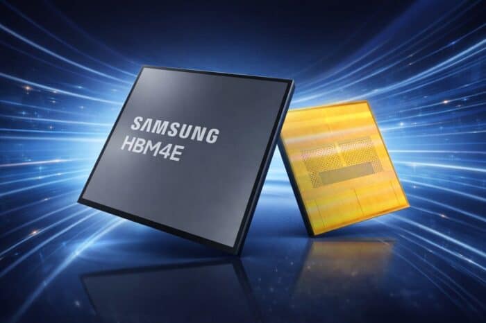
Samsung Refines HBM4E With 41% Power Efficiency Improvement
Samsung is redesigning its HBM4E memory power delivery network to tackle rising power and thermal demands in next-generation AI chips, according to TechPowerUp.
The move follows the initial rollout of Samsung’s first commercial HBM4, which operates at 11.7 Gbps with potential scaling up to 13 Gbps. As AI accelerators grow more power-hungry, memory architectures must evolve to maintain stability and efficiency at higher bandwidths.
From HBM4 to HBM4E: More power, more complexity
Transitioning from HBM4 to HBM4E significantly increases the number of power bumps from 13,682 to 14,457 within the same physical footprint.
Denser and thinner wiring raises current density and electrical resistance. As resistance climbs, voltage weakens while traveling through circuits, a phenomenon known as IR drop. The higher resistance also produces additional heat, creating a feedback loop that can affect both performance and long-term reliability.
Power network redesign on the base die
To address these challenges, Samsung reworked the internal power layout of HBM4E.
Engineers segmented the previously centralized MET4 power block on the base die. The large honeycomb-style MET4 structure was divided into four smaller sections to improve distribution efficiency.
Upper metal layers were also split to reduce routing congestion and shorten power delivery paths. By minimizing distance and resistance in these paths, Samsung aimed to stabilize voltage and limit thermal buildup.
Measured improvements
Samsung reports substantial gains with the HBM4E redesign.
The company achieved a 97% reduction in metal circuit defects compared to HBM4. IR drop performance improved by 41%, giving the memory greater voltage headroom for higher operational speeds.
These changes also enhance overall reliability, which becomes increasingly critical as AI accelerators scale toward higher power envelopes and larger memory stacks.
Looking beyond HBM4E: Separating memory and GPU
Samsung is also exploring more radical architectural changes.
One concept under investigation involves physically separating HBM from the GPU using advanced interconnect technologies. Photonic interconnects, based on optical transmission, could enable terabit-per-second data rates, potentially around 1,000 times faster than traditional copper links.
Improvements in substrate wiring may allow HBM and GPU components to sit more than 5 centimeters apart. Greater separation could dramatically improve thermal management in AI accelerator systems, where heat density continues to rise.
Samsung’s HBM4E redesign signals a broader shift in AI hardware engineering, focusing on power efficiency, scalability, and long-term reliability as demand for high-performance AI infrastructure accelerates.
In other developments, SK Hynix and SanDisk have introduced HBF memory, positioning it as a potential alternative to traditional HBM designs.
At the same time, NVIDIA’s upcoming Rubin architecture is widely expected to accelerate demand for HBM4, as next-generation AI GPUs push memory bandwidth and power requirements even further.
Read our disclosure page to find out how can you help Windows Report sustain the editorial team. Read more


Improve this guide


User forum
0 messages