NVIDIA's GeForce RTX 5090 will feature a physical monolithic die, heavily boosting its performance
This graphics card beast will have 24,567 CUDA cores
![]() 3 min. read
3 min. read
![]() Published on
Published on
Share this article
Read our disclosure page to find out how can you help Windows Report sustain the editorial team. Read more
If you’ve heard about the NVIDIA GeForce RTX 5090, you know that it’s rumored to bring a big change in graphics cards world. Many people excited because it promise very strong performance for gaming and other graphic work. This new card maybe have better speed, more memory, and advanced tech making games look super real.
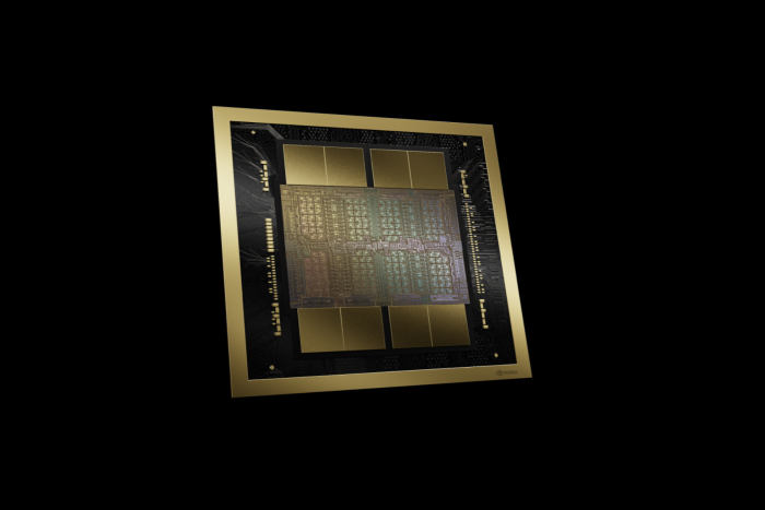
Everyone waiting to see how good it will be when come out! Let me explain. The main part of this powerful machine is the GB202 Blackwell die. It is huge and solid like one big piece. This is different from before because NVIDIA was trying chiplet designs for other chips. But for the RTX 5090, they keep to a monolithic design as NVIDIA’s Bryan Cantazaro explains in an X post:
Four years ago, we split GA100 into two halves that communicate through an interconnect. It was a big move – and yet barely anyone noticed, thanks to amazing work from CUDA and the GPU team. Today, that work comes to fruition with the Blackwell launch. Two dies. One awesome GPU.
Bryan Cantazaro, VP, Applied Deep Learning Research @ NVIDIA
Why is this new die going to bring?
Why is this important, you wonder? Well, it’s all about performance. The first specs are really very amazing. We see as many as 24,567 CUDA cores. Yes, you read that right. That’s a potential powerhouse capable of delivering unprecedented performance. The design choice is interesting because even though many in the industry are moving to chiplet designs, NVIDIA is choosing a single large piece for its top consumer GPU. This might mean better communication inside the chip and less complicated issues that can come with using multiple small chips together.
Some say they could put two GB203 dies into this big package, even if it does not officially count as a chiplet design. This method can provide benefits from both sides: the efficiency found in monolithic designs and the strength seen in chiplet designs. It’s a smart solution to solve communication delays that sometimes cause problems in systems using chiplets.
NVIDIA has done something similar in past. They have split dies and linked them together to make scalability better, but it did not become big news. The RTX 5090 might be the result of all these hard work, showing a design that is both new and very strong. Also important to mention, it will probably use the TSMC 4NP process node, expecting to give a 30% better density improvement. That’s a big deal for both performance and efficiency.
Now, let’s talk about the exciting parts of the RTX 5090. There are many rumors going around about a 512-bit interface and brand new cooling and PCB solutions to manage this powerhouse. It is clear NVIDIA goes forward strongly, especially since AMD seems to move away from very high-end graphics competition. This can give NVIDIA an open path to lead in gaming area with its Blackwell GPUs.
The launch for the RTX 5090 is much awaited, and it will probably come to stores only a few weeks after the RTX 5080. With specs like these, RTX 5090 will most likely come at a hefty price. We’ve heard about it from Wccftech.
What do you think about the new NVIDIA GeForce RTX 5090? Let’s talk about it in the comments below.


User forum
0 messages