With the new ASML machines, Intel produces silicon wafers faster than chewing gum
The new lithography technology dramatically increases silicon wafer production
![]() 1 min. read
1 min. read
![]() Published on
Published on
Share this article
Read our disclosure page to find out how can you help Windows Report sustain the editorial team. Read more
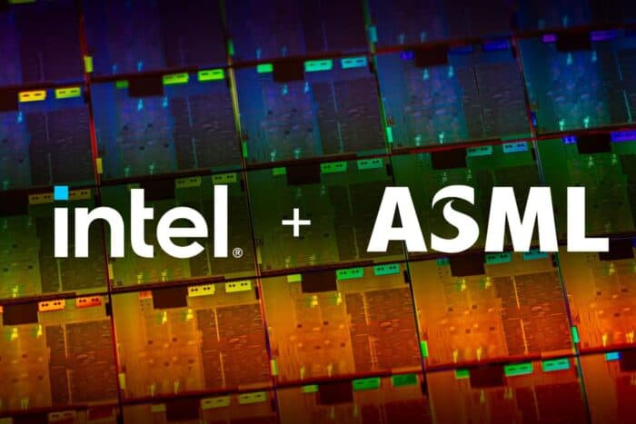
Intel has announced that its initial deployment of two advanced lithography machines from ASML Holding has entered production, demonstrating enhanced reliability over previous models. This goes back to 2022, when the two companies announced their collaboration, promising to start wafer production in 2025.
It seems that everything went according to the plans, because, as Reuters reported, according to Steve Carson, Intel’s senior principal engineer, the company successfully processed 30,000 silicon wafers in a single quarter using these high numerical aperture (NA) machines.
These machines are designed to produce smaller and faster computing chips more efficiently. Early data indicates that the new high NA machines are approximately twice as reliable as earlier generations, with the capability to perform tasks that previously required multiple exposures and processing steps in a single exposure, thereby reducing time and costs.
Allegedly, Intel will use the new machines for its upcoming 18A processor manufacturing technology and future 14A technology. Boosting the manufacturing process for silicon wafers will obviously lead to increased chip production and ultimately to higher revenue.
This coincides with Intel launching the new Xeon 6 chips for AI centers. It’s certainly a huge step for Intel to get back in the game with AMD.


User forum
0 messages